• Semiconductor Packaging

    “Persistence is the key to success!”—PrecisioNext has launched self-developed 8 inches/12 inches die bonder. We started with the underlying motion controller, servo drive, DC motor and algorithm, which are applied to our own devices. With the strong fundamental built up, we have solved the pain points of low localization of semiconductor packaging devices and long-term dependence on expensive imported equipments.
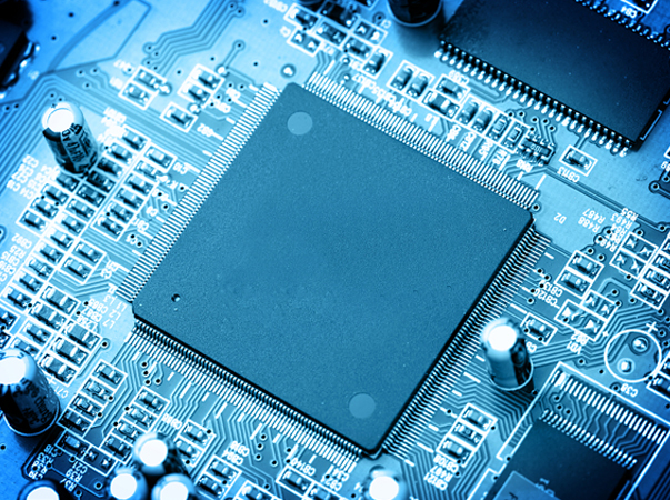
    PrecisioNext has launched IC die bonder, including DA801, DA1201, SkyBonder and so on. Our equipments’ placement accuracy can hit ±10-25μm@ 3σ, the theta placement accuracy is ±1°@3σ, this performance is competitive as compared with the high-end products in global market. Equipments advantages: flexible dual dispensing system; stable bond force control system; intelligent chip detection and compensation; user friendly interface. It is available for general IC packaging purpose, like QFN, DFN, BGA, LGA, SIP and others...
    See More >
  • Photonics Packaging

    PrecisioNext has developed ultra-high precision die bonder with 1.5μm positioning accuracy, and 3μm placement accuracy, such as DA401, DA401A and DA402. Their performances are competitive as compared with world leading products. Our products creatively use multiple wafers supported, different sizes of AB die attachment, containing automated tool changer which keeps up to 6 tools loaded in the tool turret. There is no need manual calibration with the high accurate and comprehensive PostBond data provided that can reduce the labor cost. Since the ultra-high precision die bonder products launched in semiconductor market, they have been highly recognized by those large companies like LUXSHARE, O-NET, AFA, etc. This provided a local opinion for the high precision high end 40G, 100G and 400G optical communication modules packaging equipments area, which can play an important role in China 5G optical communication industrial development. See More >
  • MiniLED Packaging

    MiniLED is a new generation of display technology. In cooperation with the Chinese Academy of Sciences and domestic LED chip enterprises, PrecisioNext creatively developed the COB flip-chip massive transfer device XBonder, an ultra-high speed die attach purposely designed for MiniLED packaging. It uses the COB flip-chip stab die bonding process, that is completely different from the traditional Pick-and-Place die bonding process. It supports minimum die size at 100μm. In addition, the maximum UPH can reach 180K while the placement accuracy is ±15μm@3σ. PrecisioNext Xbonder is the world-leading equipment. Therefore, with the launch of XBonder, the plateau of mass production in the MiniLED division we are facing will be solved. See More >
  • Power Devices Packaging

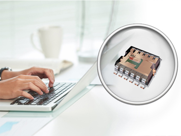
    More advanced packaging processes and technologies are chosen due to the high demands on the power device semiconductor that allowed working in high current and high voltage conditions. Clip bonding is used to replace wire bonding with its advantages in low resistance, inductance and heat impedance. Modular packaging is another advanced technology. PrecisioNext Clip Bonder power semiconductor packaging line provides an all-in-one solution for diode, transistor, MOSFET and power management IC, it includes die bonding, clip bonding and reflow soldering in one product station. The performance has been recognized by PINGWEI, CR MICRO and other industrial partners. See More >
  • Advanced Packaging

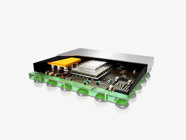
    As the chip manufacturing process reaches its physical limit, Moore’s law begins to fail. The progress of semiconductor manufacturing technology will gradually shift its focus from the front end to the back end, resulting in the development of various advanced and high-precision packaging processes. With the popularity of advanced packaging, such as SiP and 3D packaging, higher requirements are put forward for the die attach performance, such as high precision, stable bond force control, temperature field and deformation control, etc. Our high precision die attach has been widely used in SiP modules, optical modules, silicon optical devices, and other packaging products, providing domestic substitutes for advanced packaging equipment. See More >
Leave Your Message
Leave Your Message

  • Return to the top

  • +86-769-26622766-816

  • Scan the code to open mobile website

  • Scan the code by WeChat to follow us