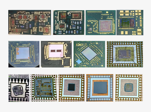
As the chip manufacturing process reaches its physical limit, Moore’s law begins to fail. The progress of semiconductor manufacturing technology will gradually shift its focus from the front end to the back end, resulting in the development of various advanced and high-precision packaging processes. With the popularity of advanced packaging, such as SiP and 3D packaging, higher requirements are put forward for the die attach performance, such as high precision, stable bond force control, temperature field and deformation control, etc. Our high precision die attach has been widely used in SiP modules, optical modules, silicon optical devices, and other packaging products, providing domestic substitutes for advanced packaging equipment.

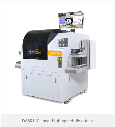
 Recommended Device
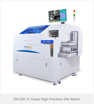